AKHAN’s manufacturing process produces the perfect diamond wafers needed for electronic production which can be used as a platform for fabricating the semiconductor devices.
August 15, 2019
By Adam Khan, Founder & CEO, AKHAN Semiconductor
The ongoing mission to create electronic devices that are smaller, more powerful and more energy-responsible has led us to the new frontier of Wide Bandgap (WBG) semiconductors. Their ability to operate at temperatures of over 300 degrees, handle 10 times higher voltages and operate with over 90 percent increased power efficiency presents the potential to save billions of dollars in energy and cut the cost of electronics when implemented.
That said, the benefits of using WBG semiconductors comprised of a material that can augment their already impressive capabilities will result in even better electronics. Historically, silicon has been the predominant material used for semiconductors, but we’ve since reached its physical limitations for both computing and powering applications. Today’s applications require lithography feature sizes that are close to the atomic limit for silicon in computing, as well as higher blocking voltages, switching frequencies, power reliability, and efficiency.
Diamond’s inherent properties have kept it at the forefront of the search to find a superior successor material. However, as the least mature option for WBG semiconductor materials, there are a number of challenges to overcome to enable widespread applicability and high-volume usage.
AKHAN was founded on the premise that diamonds are the most ideal material for this application, and we have made it our life’s work to discover and perfect a method that would refine them into a cost-efficient and effective solution across all major industries. This led to the development of our Miraj Diamond® Platform.
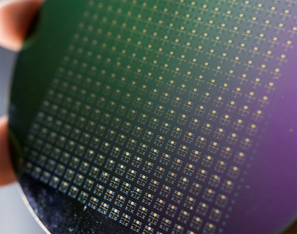
Through extensive research and scientific advancements, we created a state-of-the-art manufacturing process using methane gas and plasma as source materials, enabling us to produce these crystals at a low-cost. These wafer scale processes utilize chemical vapor deposition (CVD) reactors to form diamond in nanocrystals below 400°C, which enables their integration with complementary metal oxide semiconductor (CMOS) devices, commercial display glass and other materials previously ruled out due to temperature sensitivity, resulting in perfect diamond wafers needed for electronics.
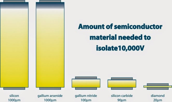
Diamond has the uncommon ability to isolate massive voltages with a small fraction of the material.
The ability to create lab-grown diamonds at a steady rate for use within electronics is ushering in a new era of smaller, faster devices that is only possible with diamond technology. Benefits of implementing diamond semiconductors include:
Diamond technology will revolutionize a number of different industries, with the most notable opportunities within automotive technology, the aerospace and defense industry, and consumer electronics. Examples of various applications include:
The diamond age is here—prepare for a world with faster, smaller, more energy efficient and affordable electronics. A more advanced world that is only possible with diamond technology.

Adam Khan
Adam Khan – Founder, Chairman, & Chief Executive Officer
Adam Khan has authored several patents and technical publications and is also a frequent speaker on Diamond Semiconductor & Clean Technology. As a result of his award-winning research, which he began as an electrical engineering student at age 19, Adam is inventor of the Miraj Diamond® Platform. Adam has also served as a speaker and expert witness to a variety of Federal bodies, including the U.S. House Space, Science, & Technology Committee and the U.S. Department of Energy. Additionally, Adam’s work was recognized and individually honored by the United States Congress in the 114th Congressional Records & Proceedings. Adam’s professional affiliations include the Materials Research Society, Board of Directors for the Chicago Council on Science and Technology, and the U.S. Council on Competitiveness. Adam earned his B.S. in Electrical Engineering and Physics from the University of Illinois Chicago, before pursuing graduate research at the Stanford University Nanofabrication Facility. He has been everything from a CleanTech Open Midwest Innovation Summit winner, a Forbes 30 Under 30, to a Modern-Day Nikola Tesla in the International Documentary Film ‘Tesla’s Children’ (2016).
Contact: info@akhansemi.com

Forging the Next 250 Years: Powering the Next Era of American Manufacturing
As manufacturers offer more customization than ever before, managing product complexity has become a critical challenge. Tune in with Dan Joe Barry, Vice President of Product Marketing at Configit, who explores how companies are tackling the growing number of product configurations across engineering, sales, manufacturing, and service. He explains how Configuration Lifecycle Management (CLM) helps organizations maintain a single source of truth for configuration data. The result: fewer errors, faster quoting, and the ability to deliver customized products at scale.
Get In Touch
Google news and SEO compliant, Industry Today’s state-of-the-art digital media platform offers bespoke media campaigns that target key decision makers and buyers to achieve your marketing and promotional goals.
![]()
Contribute
Showcase your brand and promote your business to our highly targeted audience. We offer detailed Google Analytics with measurable ROI to assure success. Submit your content for review by our Editorial team who will contact you to discuss the project further.
About Us
Reach Your Targeted Audience and Grow Your Business. Learn more About Industry Today.
Contact Us

© 2026 Industry today. All Rights reserved.