By Alain-Serge Porret, Vice President, Integrated & Wireless Systems, CSEM
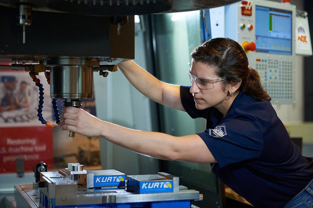
For much of the past two decades, the global semiconductor production conversation has been dominated by scale. Success has been measured in billions of dollars invested, square meters of cleanroom space erected, transistor counts, and megawatts consumed. Governments and corporations alike have competed to build ever-larger fabrication facilities, supported by massive subsidies and increasingly concentrated supply chains.
This model has delivered extraordinary technological progress, such as developments in large language models (LLMs) that have changed how we work, but it has also created an industry in which participation at the leading edge is limited to a shrinking number of players. As the cost of advanced manufacturing nodes rises into the tens of billions, many regions and companies are discovering that chasing scale is no longer a viable or even desirable strategy. In fact, corporate AI investment is projected to have reached $252.3 billion in 2025 alone, according to Stanford University; a 50% increase from the previous year.
But now a different reality is emerging, one shaped by those who can extract more value from fewer resources, refine processes instead of expanding footprints, and design chips that deliver high performance under tight energy and material constraints.
Few countries are doing this better than Switzerland. Over the past several years, the nation has shown how focusing on production of precise, efficient and specialized chips with limited and refined functions can save on costs and provide new opportunities.
As global investment dynamics shift and energy considerations become central to industrial strategy, this approach is proving to be an increasingly pivotal linchpin to the future of chip production worldwide.
The economics of advanced semiconductor manufacturing are becoming increasingly challenging. As computing, energy and infrastructure needs push the limits of what is possible today, every step forward demands exponentially higher capital investment. At the same time, geopolitical tensions, export controls, security concerns, data sovereignty and supply-chain fragmentation are adding layers of complexity and risk.
For many countries and companies, the promise of “catching up” through massive investment is giving way to a more sober assessment. Even if there was a possibility to earn the massive private or public investment, not all regions are equipped with the resources needed to generate that level of chip production. At the same time, energy consumption has become a critical constraint. Large fabs and data centers demand enormous and continuous power supply placing pressure on national grids and raising sustainability concerns.
These pressures are forcing the industry to ask a fundamental question: Is bigger always better? Or is the next phase of semiconductor innovation about learning how to do more with less?
Switzerland’s answer has long been clear. Rather than pursuing maximum scale, Swiss research institutions and industrial partners, such as CSEM, have focused on process refinement across the entire semiconductor value chain.
This approach revolves around the idea that performance is not defined solely by production scale. Architectural efficiency can ensure that more precisely designed chips have just as much of an impact as those with more generalized approaches.
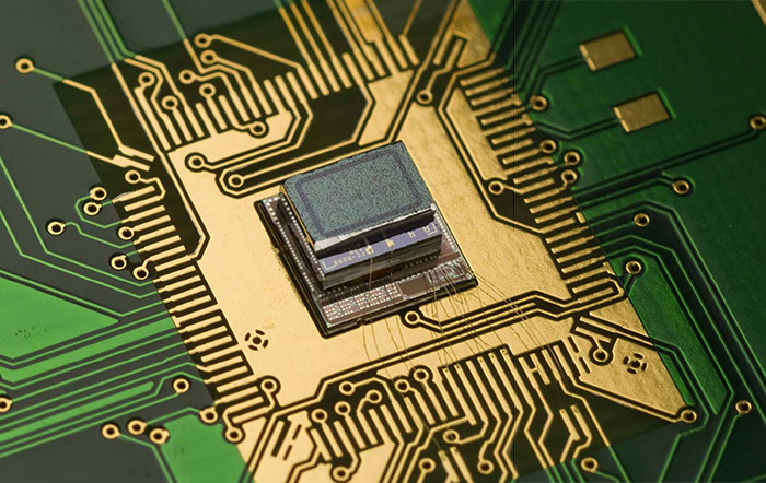
In practice, this means designing application- specific integrated circuits (ASICs) that are precisely matched to their intended workload. Low-power edge AI accelerators, for example, can deliver exceptional performance per watt by eliminating unnecessary general-purpose logic and focusing computation exactly where needed the most and nowhere else.
Refining processes also means rethinking how chips are manufactured and deployed. This philosophy stands in contrast to a scale-driven model that prioritizes throughput and density above all else. It suggests that innovation in process design can be just as transformative as innovation in fabrication scale, and often more accessible.
One of the clearest signals of this shift is the growing importance of low-power chip design. As AI and sensing capabilities are under greater demand, chips must operate in environments where energy is limited, intermittent, or expensive.
Swiss work in ultra-low-power electronics and embedded AI illustrates how deeply energy considerations can help to beneficially shape design decisions. By treating power budgets as primary constraints rather than secondary optimizations, engineers can create systems that are more precise and focused, and subsequently more effective in their limited structures.
Examples include:
These designs are not merely incremental improvements. They represent a different way of thinking about what a chip is for and how it should behave in the world. They also don’t serve as a replacement for the more generalized chips that power LLMs but rather provide functions that augment those same functions.
As energy costs rise and sustainability becomes a strategic priority, low-power capability is moving from a niche route to a central design objective. Regions and companies that master this discipline will be better positioned to deliver effective and important solutions without unsustainably scaling their infrastructure.
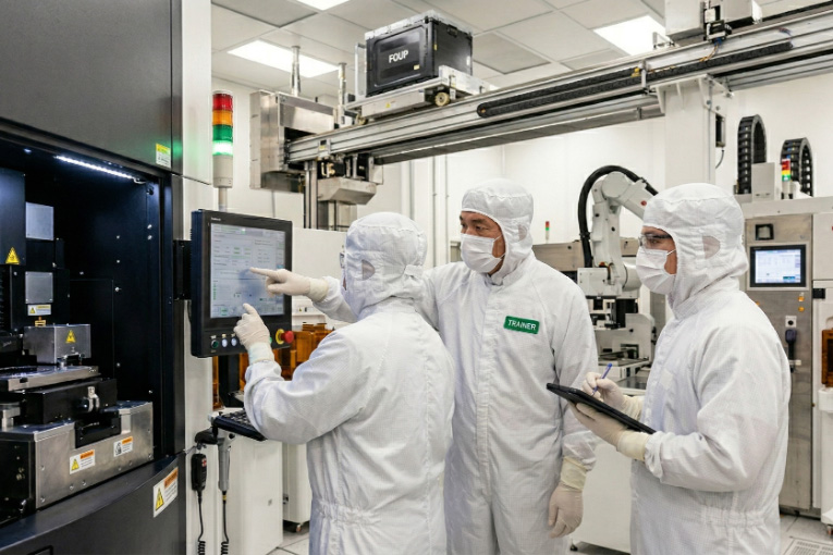
For regions that cannot invest tens of billions into large manufacturing facilities, this shift presents a meaningful opportunity. The semiconductor industry does not require uniform participation at every layer. Instead, it increasingly depends on specialized excellence at key points in the value chain.
These sorts of organizations in Switzerland demonstrate how a country can remain globally competitive in chip production without having to overcome massive hurdles like energy limitations or resource demands. By focusing on design innovation, specialized process knowhow, and close collaboration with manufacturing partners, it is possible to influence outcomes far beyond traditional scopes.
This model is particularly relevant for:
Rather than competing head-to-head with the largest players, these actors can contribute by developing technologies that complement high-volume manufacturing, simultaneously improving efficiency, reducing energy demand, and enabling new classes of applications.
The next phase of global chip production is set to be much more diversified than the last. While large-scale fabs and advanced nodes will remain essential for certain applications, they will no longer define the entire industry’s trajectory. Process innovation, architectural efficiency, and low-power design will play an increasingly decisive role. This will not only make sure that design needs are met but also provide opportunities for a wider range of developers and fabricators to take part in production.
Switzerland’s success in carving out the more precise path offers a valuable lesson, showing how the industry does not need the biggest facilities in order to have the greatest impact on the future of semiconductors. By refining processes, embracing specialization, and designing for efficiency from the outset, it is possible to deliver chips that meet real-world needs while remaining economically and environmentally sustainable.
For the global electronics and manufacturing community, the takeaway is clear. The race ahead is not simply about who can invest the most, but about who can design the smartest systems within realistic constraints. As energy demands and the need for resilience bump against rising costs, the industry may find that its most important breakthroughs are likely not coming from building bigger, but from building better.

About the Author:
Alain-Serge Porret holds the position of Vice President for Integrated and Wireless Systems at CSEM. His team provides optimized, application-specific solutions to minimize energy and footprint of autonomous connected devices and smart vision systems including technologies for wireless communication, sensing and remote powering and secure embedded software. As needed, the proposed solution can be optimized by building a dedicated application-specific integrated circuits (ASIC).
Before his current role, he co-founded several start-ups in the consumer electronics domain during a 13-year stint in Silicon Valley. His academic accolades include a Ph.D. from EPFL (Switzerland), where his work made a significant contribution to the then-emerging field of ultra-low-power CMOS radio chips.
The Rise of American Manufacturing: A New Industrial Era
As manufacturers offer more customization than ever before, managing product complexity has become a critical challenge. Tune in with Dan Joe Barry, Vice President of Product Marketing at Configit, who explores how companies are tackling the growing number of product configurations across engineering, sales, manufacturing, and service. He explains how Configuration Lifecycle Management (CLM) helps organizations maintain a single source of truth for configuration data. The result: fewer errors, faster quoting, and the ability to deliver customized products at scale.
Get In Touch
Google news and SEO compliant, Industry Today’s state-of-the-art digital media platform offers bespoke media campaigns that target key decision makers and buyers to achieve your marketing and promotional goals.
![]()
Contribute
Showcase your brand and promote your business to our highly targeted audience. We offer detailed Google Analytics with measurable ROI to assure success. Submit your content for review by our Editorial team who will contact you to discuss the project further.
About Us
Reach Your Targeted Audience and Grow Your Business. Learn more About Industry Today.
Contact Us

© 2026 Industry today. All Rights reserved.